Clocking
This section describes how and where clock signals are routed. Switches symbolize connections that can be altered by placement of capacitors. Default connection is symbolized by switch position.
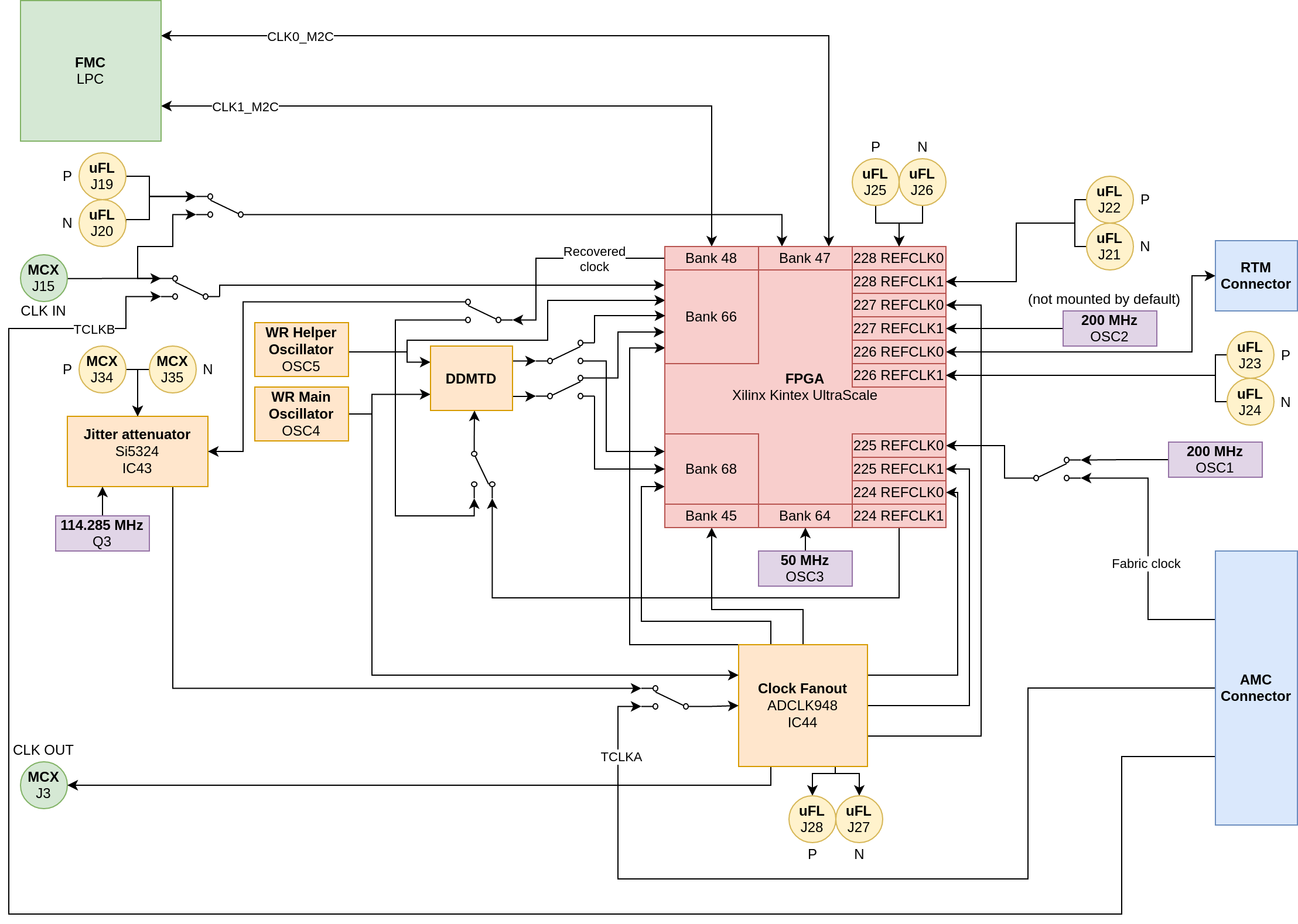
FPGA Oscillators
OSC1 - 200 MHz clock for MGT
OSC2 - 200 MHz clock for MGT (not mounted by default)
OSC3 - 50 MHz main clock source for FPGA resources
Clock distribution
Sayma cards recover their DRTIO clock from the backplane’s transceiver link or - if they are stand-alone – from their SFP/SATA transciever link. DRTIO documentation is here.