PCB technical information
Stackup:
Layer |
Copper [um] |
Function |
|---|---|---|
L1 |
36 |
polygons, short traces and analog signals between DAC and connectors |
P2 |
18 |
GND |
L3 |
18 |
high speed signals, LVDS, GTX, clocks |
P4 |
18 |
GND |
L5 |
18 |
high speed, LVDS, GTX, clocks, vertical slow control |
P6 |
18 |
GND |
L7 |
18 |
I2C, SPI, mezzanine IOs, status, LED, power polygons |
P8 |
18 |
GND |
P9 |
18 |
split power plane |
L10 |
36 |
short signal layers (ADCs), mainly polygons and short traces (EMI mitigation) |
The total height of the board is: 1.59 mm. Dielectric is a standard FR408.
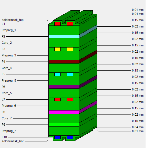
SAYMA RTM stackup
Note
The thickness of copper in Figure 17 is 0.04mm and 0.02mm is due to approximation. In fact it is 0.036mm and 0.018mm. See table above.